Inverters are circuits that convert dc power into ac power at desired output voltage and frequency. The inverters achieve this by using thyristors as switches and hence circuits with fewer components have non-sinusoidal output waveform. By adding circuit complexity, nearly a sinusoidal output voltage is possible to obtain.
Depending upon commutation circuits i.e., some external means that are needed to forcefully turn OFF the thyristor. The inverter circuits are classified broadly as,
- Parallel Inverter,
- Series Inverter,
- Bridge Inverter.
- Half Bridge Inverter, and
- Full Bridge Inverter.
- Half Bridge Inverter, and
- Full Bridge Inverter.
In the last article, we have learned about half-bridge inverters. The main problem of a half-bridge inverter is the requirement of a 3-wire dc supply. This drawback can be eliminated by using a full-bridge inverter. In this article, let us learn about the full-bridge inverter with circuit diagrams and waveforms.
Full Bridge Inverter With R Load :
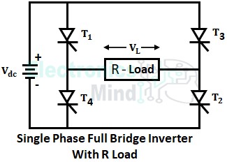
The below figure illustrates the single-phase full-bridge inverter circuit using thyristors as switching devices. Here the inverter circuit uses four thyristors divided into two pairs (T1, T2, and T3, T4). One pair of devices operates simultaneously.
Working of Full-Bridge Inverter With R Load :
In the above circuit diagram, the commutating circuit of the thyristors is not shown for simplicity. Assume that on removing gate pulses to the thyristors they are turned OFF. The full-bridge inverter operates in two modes in one cycle of ac voltage at the output side.
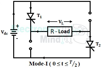
- Mode-I : During the interval between 0 and T/2 i.e., for 0 ≤ t ≤ T/2, thyristor pair T1 and T2 are triggered and they start conducting. When T1 and T2 are turned ON, the load voltage follows the positive source voltage Vdc. At the instant t = T/2, the triggering pulses are removed for both the thyristors T1 and T2 and are turned OFF.
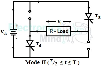
- Mode-II : At the same time i.e., at t = T/2, when T1 and T2 get turned OFF, the triggering pulses are given to thyristor pair T3 and T4. This pair will conduct for the interval between T/2 and T (for T/2 ≤ t ≤ T) and the load voltage follows the negative source voltage -Vdc as shown below.
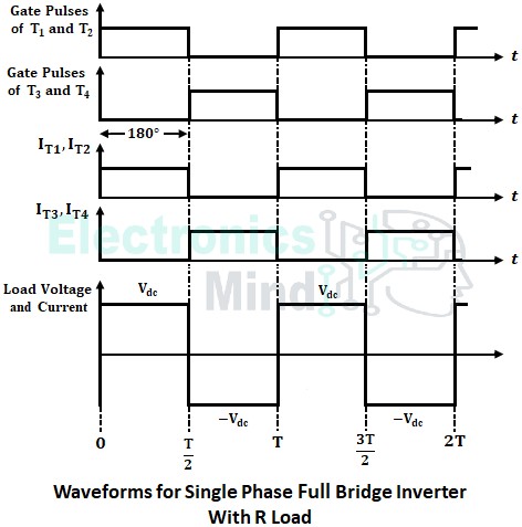
The thyristor pair T3, T4 conducts until thyristor pair T1, T2 have triggered again at t = T, and the cycle repeats. The below shows the waveforms of gating signals, output voltage, and currents of thyristors and diodes. Since load is assumed to be purely resistive, the load current will be equal to load voltage.
From the above two modes, we can observe that the direction of current flowing through the load in mode-I is opposite to the current flowing through the load in mode-II. The thyristor pair T1, T2 conduct for time period 0 to T/2 for producing positive half cycle, and thyristor pair T3, T4 conduct for time period T/2 to T for producing negative half cycle. Thus an alternating output is obtained at the output side from a dc power.
Full Bridge Inverter With RL Load :
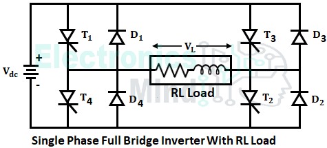
In the above operation of the full-bridge inverter, we know that load connected is of resistive type. But generally, in practice, most of the loads are resistive-inductive (RL) type. Now let us see the operation of a full-bridge inverter with RL load. The below shows the circuit diagram of a full-bridge inverter with RL load.
Compare to the circuit diagram with resistive load, in this circuit, two extra diode pairs (D1, D2, and D3, D4) are used. The four diodes are connected in anti-parallel to the four thyristors. The purpose of diodes is discussed below in working.
Working of Full-Bridge Inverter With RL Load :
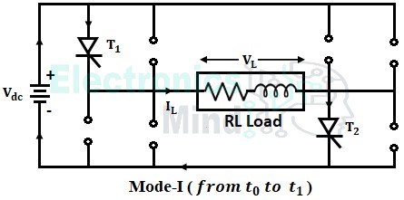
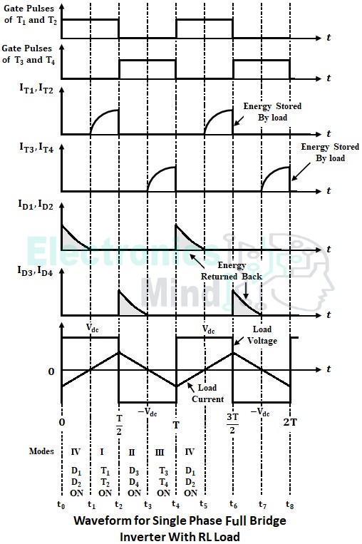
The operation of a full-bridge inverter with RL load can be better understood by considering four modes,- Mode-I : In mode-I, thyristors T1, T2 are triggered at instant t = t0, but these thyristors will not turn ON as these are reverse biased by the self-induced negative voltage across the inductive load. Due to this negative inductive load current, diodes D1 and D2 are forward biased and provide a path to feed it back to the source. The thyristors T1, T2 will start conducting from t = t1 once the negative load current becomes zero. Again the load current flows in the positive direction and increases from zero to Imax, and the load voltage follows the positive source voltage Vdc.
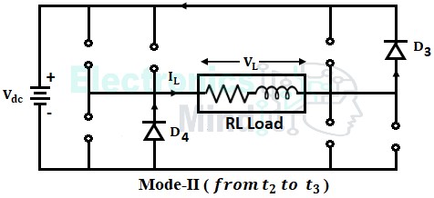
- Mode-II : At instant t = t2, the triggering pulses are removed from T1, T2 and are given to T3, T4. Now, T3 and T4 are triggered, but these thyristors will not conduct as these are reverse biased by the self-induced positive voltage across the inductive load. The inductive load develops a large voltage, by releasing its stored energy in mode-I. Due to this, diodes D3 and D4 are forward biased, and the positive load current stored is fed back to the supply through diodes D3 and D4 as shown below.
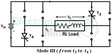
- Mode-III : At t = t3, the stored energy in the inductor becomes zero. Hence, thyristors T3 and T4 start conducting, and the load current starts flowing in a negative direction through the path shown below and increases from zero to -Imax.
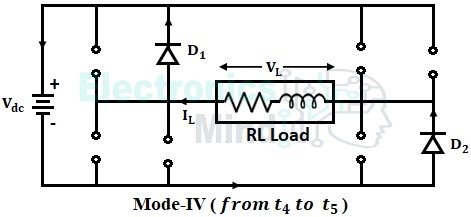
- Mode-IV : At t = t4, the triggering pulses are removed from thyristors T3, T4, and given to T1, T2. But T1, T2 don’t start conducting due to inductive load which does not allow a sudden change in current. Thus the load current doesn’t become zero instantaneously and it starts releasing stored energy in mode III through diodes D1 and D2 as shown below.
At t = t5 the load current due to inductance becomes zero and thyristors T1, T2 will start conducting. From t5 the cycle repeats i.e., the whole operation from mode-I to mode-IV will repeat. The waveforms of load current and voltage with RL load are shown below.
From the above waveforms, when an inductive load is connected to the inverter, the load current lags behind the load voltage. The function of diodes is to feed the reactive power back to the source provided the load is inductive. These diodes are called fed back diodes. However, if the load is purely resistive reactive power will be zero and hence the need for diodes is eliminated.
The triggering pulses applied for both the thyristor pairs T1, T2, and T3, T4 differ in phase by 180°. The frequency of output voltage is the same as that of a half-bridge inverter i.e., frequency = 1/T, but the magnitude is doubled. Just like a half-bridge inverter, the output frequency can be controlled by varying the time period T.
Care must be taken to see that the thyristors present in the same branch of the full-bridge inverter do not conduct together. If both the thyristors are triggered simultaneously, it leads to a severe short-circuiting to the source.

