Necessity of Snubber Circuit :
For the reliable operation of an SCR, it should be ensured that the current and voltage ratings of the SCR should not exceed their rated values. In case, if due to any abnormal condition, SCR is subjected to over voltage or over current then, it may be damaged. Therefore, SCR’s must be protected from high values of overvoltages and overcurrents. Also, SCR’s are the most sensitive devices. The SCR’s or thyristors are subjected to internal and external overvoltages.
Internal Overvoltages :
Internal overvoltages are caused by the thyristor operation (i.e., during commutation of thyristor). When the thyristor is switched ON by applying a positive gate signal, the conduction begins at the location which is near the gate. After a fraction of a second, the conduction area increases and spreads to the complete area of the junction.
Now if the rate of rise of anode current (di/dt) is higher when compared with the spreading velocity of carriers across the cathode junction. Due to high current density, it leads to the formation of hot spots near the gate connection which in turn increases the temperature of the SCR. If in case the temperature increases the maximum possible limit, it may result in permanent failure of SCR.
External Overvoltages :
External overvoltage is caused mainly on the load circuit or on the supply lines i.e., external overvoltages are caused due to lightning strikes on the lines feeding the thyristor system or due to interruption of current flow in an inductive circuit. If the rate of rise of forward anode voltage exceeds the specified maximum limit, then it causes switching from OFF state to ON state. It can also be said that if (dV/dt) increases beyond the specified value, then it leads to false triggering of thyristor which is undesired.
Therefore, thyristors must be protected from high values of overvoltages and overcurrents. Since thyristors are not sensitive devices and if they have not been protected then along with thyristor other components of the circuit may get damaged.
A snubber circuit is a protective circuit used to protect the SCR from false triggering and transient overvoltages. It basically consists of a capacitor and a resistor connected in series. We know that SCR is a controllable device, i.e., the turning-ON and turning-OFF of an SCR is controllable through a gate signal.
Now, if SCR is falsely triggered at some undesirable instant, this will lead to malfunctioning of SCR and hence the output will be undesirable. Also, the transient overvoltages will be so high that they may completely damage the SCR and the whole circuit. Hence, in order to protect the SCR from the above two undesirable conditions, a snubber circuit is used.
Working of Snubber Circuit :
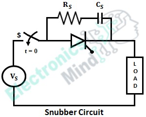
The below shows the circuit of Snubber circuit. The working of the snubber circuit can be explained by explaining the functions of the two elements present in it, i.e., by explaining the function of the resistor and the capacitor.
Function of Capacitor :
Suppose at t = 0, the switch shown in the above figure is closed. Exactly at t = 0, the capacitor acts as a short circuit (zero voltage) owing to its property. As the SCR is connected in parallel with the capacitor, the same zero voltage appears across it instead of the full supply voltage. After some time the voltage across the capacitor increases slowly and gradually picks up the full voltage.
Hence, from the above analysis, it can be said that the supply voltage does not appear instantaneously across the SCR (because of the capacitor), rather it builds up at a slow rate. Hence, the SCR is protected from transient overvoltage and also prevented from false triggering.
Function of Resistor :
The function of the resistor is to prevent the inrush of current through the SCR when it is triggered. When the SCR is in blocking mode, the capacitor charges to the full supply voltage. After the SCR is triggered, a closed-loop will be formed by the capacitor and SCR. Due to the presence of the voltage across the capacitor, due to the closed path, the capacitor discharges. Due to this, a sudden high current flows through SCR. Therefore, the resistance path of SCR is very low.
Now, when the resistor is used in series with the capacitor, the closed path will be formed by, Rs Cs and SCR. Thus the discharge current will be equal to Vs/Rs which will be very less when compared to the previous value. Hence, the resistor in series with the capacitor protects the SCR from the high value of di/dt.
Design of Snubber Circuit Parameters :
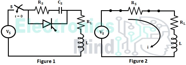
The below figure shows the snubber circuit connected across the SCR. At t = 0, the switch is closed and hence the capacitor acts as a short circuit as shown in the second figure.
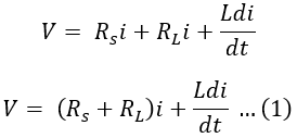
As the SCR is not yet triggered, it acts as an open circuit. Now the circuit equation in this condition is given as,
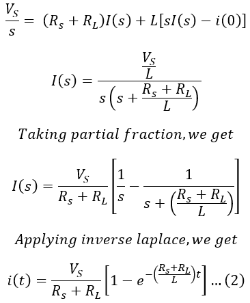
Applying Laplace to equation (1), we get,
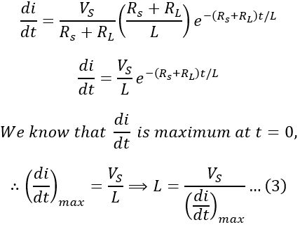
Differentiating equation (2) with respect to ‘t’, we get,
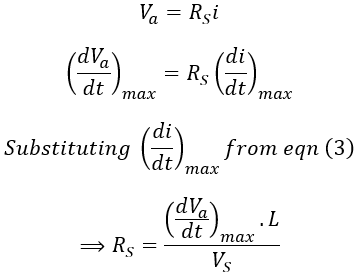
The voltage across the SCR is given by,
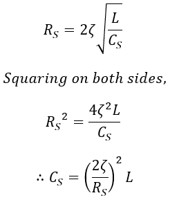
The snubber circuit shown above is always designed for critically damped conditions. Hence, for a critically damped circuit,
Where ζ is the damping ratio.

nice article