What is Boost Converter?
A boost converter is basically a step-up chopper or step-up dc-to-dc converter by which we can obtain an output voltage greater than the input voltage. In other words, boost converters are regulator circuits that generate a voltage at the output side whose magnitude will be greater than or equal to the input applied voltage.
In many domestic and industrial applications, there is a requirement for conversion of DC voltage source to different levels. Thus there is a need for a dc-to-dc converter that converts a fixed-voltage dc source into a variable-voltage dc source.
A DC chopper is a static device by which we can obtain variable dc voltage from a source of constant dc voltage. It is similar to a function of an AC transformer used to step up or step down the dc voltage source. Besides saving in power, the dc chopper offers various advantages like high efficiency, fast response, compact in size, easy and smooth control, low maintenance, low cost, etc.
Circuit Diagram of Boost Converter :
The circuit diagram of the boost converter using power MOSFET as a switching device is shown in the below figure. It consists of an inductor connected in series after which a power MOSFET is connected in parallel with the positive and negative terminals.
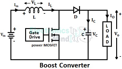
A diode is connected in series with the load after the power MOSFET which also acts as the switch by automatically forward biasing and reverse biasing. A capacitor in parallel is placed at the load side for removing ripples in the output signal.
The high-speed ON/OFF semiconductor switch (power MOSFET) will alternatively connect and disconnect the load from the supply at a rapid rate so that a voltage of higher magnitude than the input voltage will appear at the output side. The semiconductor switch (power MOSFET) is turned ON and OFF by controlling the gate terminal using Pulse Width Modulation(PWM).
Working of Boost Converter :
By using a boost converter we can obtain an output signal greater than the input signal. Initially, the power MOSFET is turned ON by applying a signal at the gate terminal. Now the supply current (Iin) starts flowing through the inductor (L) and power MOSFET as shown below.
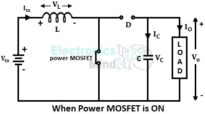
Once the power MOSFET is switched ON, the inductor current (IL) starts increasing and it will charge with a polarity according to the direction of the flow of supply current as shown above. The inductor current rises linearly from minimum to maximum value.
The diode is reverse biased due to stored energy in the capacitor which appears across the cathode (anode is at zero potential due to the conducting power MOSFET). Thus the reverse biased diode will isolate the load from the supply. If the capacitance is very high, the capacitor supplies a constant load current.
Now when the power MOSFET is switched OFF, the supply current which was flowing through the inductor, and power MOSFET will now flow through the inductor, diode, capacitor, and load as shown below.
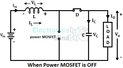
When the power MOSFET is switched OFF, the charged inductor will start discharging with reversed polarity due to which the diode gets forward biased. The load now receives a voltage from the supply along with the inductor voltage (i.e., Vin + VL) and the capacitor will be charged.
The inductor current will fall linearly until the power MOSFET is turned ON again. Therefore we can observe that the load receives a voltage (average value) greater than the input voltage, hence the name boost. The associated voltage and current waveforms for the operation of the boost converter are shown below.
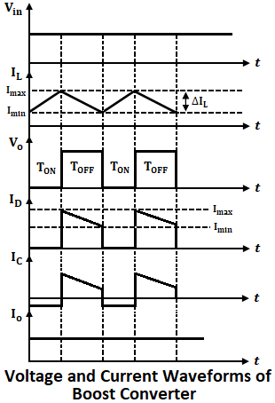
In the above waveforms, there are two periods TON and TOFF. TON is the period for which the power MOSFET is turned ON and TOFF for which power MOSFET is turned OFF. We can see that during the TON period of MOSFET, output voltage Vo will be zero, IL will increase from imin to imax, and current at the diode ID will be zero.
In TOFF period of MOSFET, output voltage Vo will be due to supply and inductor. Once MOSFET is OFF, IL will start falling to imin, and ID will be equal to IL. On applying KVL to the circuit when MOSFET is in OFF state, we will get,
The energy supplied to the inductor during the ON period of MOSFET is given as,
Also, the energy supplied by the inductor during the OFF period of MOSFET is given as,
For a lossless circuit WON = WOFF,
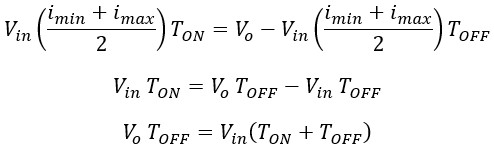
We know that T = TON + TOFF,
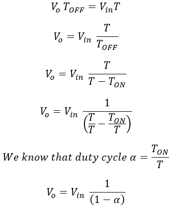
From the above equation, it is clear that the average output voltage can be controlled by controlling the duty ratio. For α = 0 to 1, the output voltage will be equal to or greater than the input voltage i.e., Vo ≥ Vin, thus stepping up the voltage.
Due to the use of a single power MOSFET, the boost converter has high efficiency. However, the power transistor has to sustain high peak currents.
Applications of Boost Converter :
The applications of boost converter are,
- Consumer electronics,
- Regenerative braking of dc motor,
- DC motor drives,
- Communication applications operated by batteries,
- Battery power systems.